Key Features
- Frequency Range LF - 18 GHz
- SlopeSwitchable
- Low Loss 1 dB
- Supply Single
- compact size3x3 mm
Applications
- Wideband Receivers
- SDR
- Test Equipment
- Telecommunication
Architecture
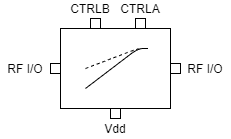
ATEK900N3 Block Diagram
ATEK900N3 is a wideband 2-bit Gain Equalizer with Switchable Gain Slope. Frequency of operation goes down to Low Frequency close to DC and goes up to 18 GHz. ATEK900N3 operates with positive supply voltage and states are set by positive voltage control interface. Eliminating the need for external negative bias circuitry. RF Input and output are matched to 50 ohms internally. This allows users to easily integrate the equalizer to wideband circuits. Equalizer is housed in compact 3x3 mm low cost SMD package. Evaluation Board, bare die, custom package, and module options are available upon request.
Technical Specifications
| Parameter | Condition | Min | Typical | Max | Unit |
|---|---|---|---|---|---|
| Frequency Range | LF | 18 | GHz | ||
| Insertion Loss | 0.01 GHz | 0.45 | dB | ||
| 2 GHz | 0.6 | dB | |||
| 6 GHz | 0.6 | dB | |||
| 12 GHz | 0.8 | dB | |||
| 18 GHz | 2.1 | dB | |||
| Input Return Loss | 18 | dB | |||
| Output Return Loss | 17 | dB | |||
| Input P1dB | TBD | dBm | |||
| Input IP3 | 34 | 40 | dBm | ||
| Switching Time | On | TBD | 250 | ns | |
| Off | 250 | ns | |||
| DC Supply Voltage | 5 | V | |||
| Current consumption | 2.5 | mA | |||
| Control Level | Low | 0 | V | ||
| High | 5 | V | |||
| Operating Temperature | -40 | 85 | °C |
Available Resources
Ready to Integrate ATEK900N3?
Contact our engineering team for technical support, samples, or volume pricing.
Request More Information