
Company Overview
High-Performance RF & Microwave Expertise
ATEK MIDAS combines deep technical expertise with proven innovation to deliver high-performance RF semiconductors and integrated solutions for demanding applications.
Company Overview
ATEK MIDAS combines deep technical expertise with proven innovation to deliver high-performance RF semiconductors and integrated solutions for demanding applications.
ATEK MIDAS applies novel expertise, creativity, and passion to design high performance analog, mixedsignal ASICs & RFICs and advanced GaAs & GaN MMICs & Modules for Aerospace, Automotive, Communication, Data Center, Defense, Industrial, Medical, Scientific, and Test & Measurement markets. We partner with our customers to provide focused IC design and development services delivering IP blocks to engineering prototypes to turn-key production solutions complemented by our line of MMIC standard products for communication and sensor applications to 100 GHz.

Our cross-functional team of engineers, operations, and sales collaborates easily with customers and vendors worldwide.
From our founding in 2017, ATEK is leveraging its broad technical expertise to fulfil its mission of creating a company capable of designing and manufacturing a full range of advanced analog & mixed-signal ASICs, RFICs, MMICs and modules for a diverse range of industries.
The ATEK Midas Team is highly motivated to enable next-generation solutions for our customers, by providing superior products while adhering to high quality standards.
Çifte Havuzlar Mah. Eski Londra Asfaltı Cad.
YTÜ Teknopark B2 Blok 151/1G No:105
34220 Esenler / Istanbul, Türkiye
Tel: +90 212 483 71 67
E-mail: info@atekmidas.com
Bilkent Cyberpark
Cyberplaza A Blok, 1. Kat No: 109A
Ankara / Türkiye
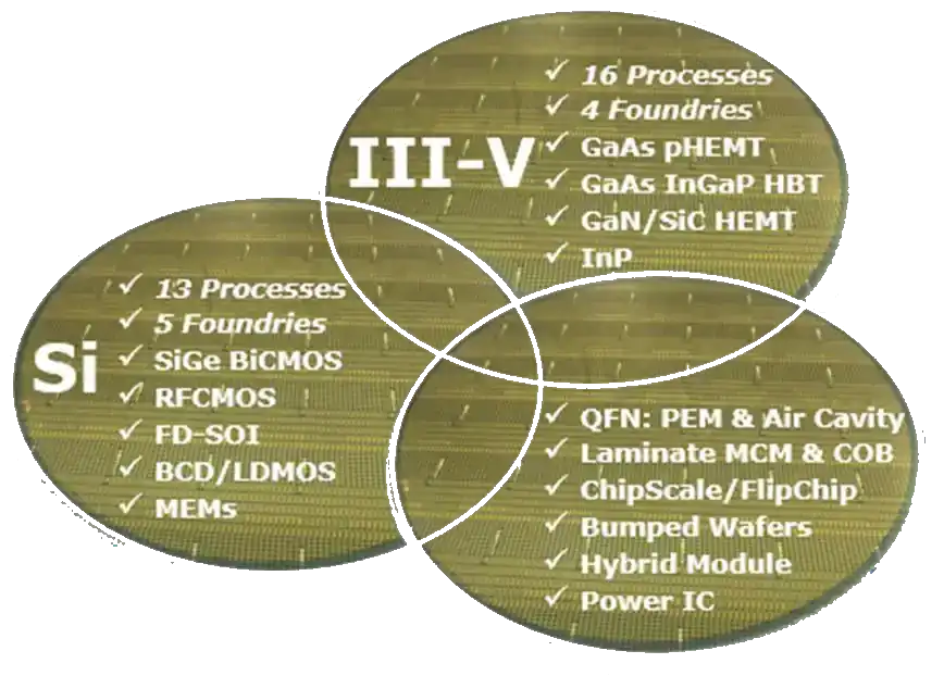
ATEK Midas is fabless, utilising world-class semiconductor technologies including SiGe BiCMOS, RF CMOS, SOI, BCD, GaAs, GaN & InP from industry-leading wafer foundries.
We leverage our portfolio of Analog, Digital, Mixed-Signal, Optical, Power, Timing & RF/Microwave core IP functional blocks. We specialise in addressing IC obsolescence and EOL risks.
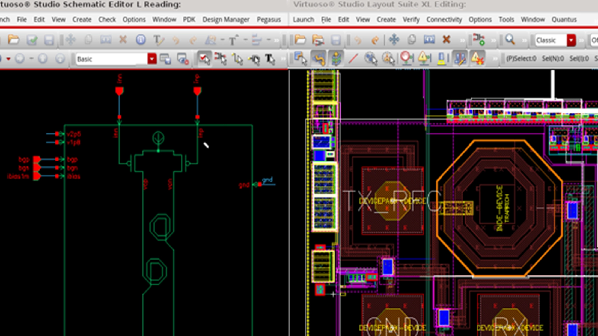
We design RFICs, MMICs, optical ICs and CDRs, ADCs and DACs, PMICs, and IP blocks across an extensive range of process nodes.
On the compound semiconductor side we work in GaAs, GaN/SiC, and InP at geometries from 0.5 µm down to 0.1 µm.
On the silicon side we cover SiGe BiCMOS, SOI, RFCMOS, BCD, and MEMs technologies from 130 nm to 3 nm.
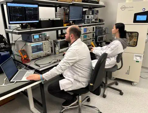
Our 400 m² (4,305 sf) design and test facility has digital, mixed-signal, and small & large signal RF measurement capability, including environmental testing from −55°C to +125°C.
We can characterise & production-test SMT packaged products as well as probe wafer/die products through 110 GHz.
We engage with high-quality wafer foundries, IC assembly, test, & screening partners to assure our customers a secure source of supply.
A disciplined, milestone-driven flow from specification through tape-out, qualification, and volume production. We manage process selection, foundry relationships, layout, verification, and supply chain so customers receive a production-ready device, not just a prototype.
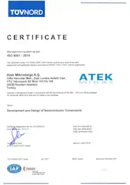
ATEK Midas embraces Quality & Continuous Improvement in everything we do. We are ISO 9001:2015 certified by TÜV.
Learn about our Quality programme →