Key Features
- Frequency Range 0.01 - 8 GHz
- Gain 18.5 dB
- Noise Figure 2.5 dB
- P1dB 17 dBm
- Supply Single
- Control Positive
- compact size4x4 mm
Applications
- Wideband Receivers
- SDR
- Test Equipment
- COMINT
- Telecommunication
Architecture
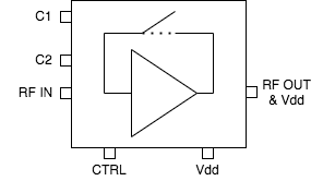
ATEK951N4 Block Diagram
ATEK951N4 is a wideband low noise amplifier with bypass option covering 0.01 to 8 GHz frequency range. Amplifier operational low frequency range can be extended to lower frequencies by increasing external component values. Amplifier provides flat gain and low noise over wideband with single supply voltage. Bypass state is controlled with positive voltage, eliminating the need for negative voltage rails. This allows users to easily realize wideband receiver frontends. Amplifier housed in compact 4x4 mm low cost SMD package, input and output matched to 50 ohms internally. Evaluation Board, bare die, custom package, and module options are available upon request.
Technical Specifications
| Parameter | Condition | Min | Typical | Max | Unit |
|---|---|---|---|---|---|
| Frequency Range | 0.01 | 8 | GHz | ||
| Gain | 0.01 GHz | 19 | dB | ||
| 1 GHz | 18.5 | dB | |||
| 3 GHz | 18.5 | dB | |||
| 6 GHz | 19.5 | dB | |||
| 8 GHz | 18 | dB | |||
| Noise Figure | 0.01 GHz | 6 | dB | ||
| 1 GHz | 2.5 | dB | |||
| 3 GHz | 2 | dB | |||
| 6 GHz | 2.8 | dB | |||
| 8 GHz | 4.5 | dB | |||
| Input Return Loss | -11 | dB | |||
| Output Return Loss | -12 | dB | |||
| Insertion Loss | Bypass State | 2.5 | dB | ||
| Input Return Loss | Bypass State | -16 | dB | ||
| Output Return Loss | Bypass State | -16 | dB | ||
| Output IP3 | 30 | dBm | |||
| Output P1dB | 17 | dBm | |||
| DC Supply Voltage | 5 | V | |||
| DC Supply Current | LNA State | 91 | mA | ||
| Bypass State | 5 | mA | |||
| Control Level | Low | 0 | 1 | V | |
| High | 2 | 5 | V | ||
| Operating Temperature | -40 | 85 | °C |
Available Resources
Ready to Integrate ATEK951N4?
Contact our engineering team for technical support, samples, or volume pricing.
Request More Information